| Bottom | Home | Article | Bookshelf | Keyword | Author | Oxymoron |

$\frac{1}{2}$

Basics of the Semiconductor Industry

Cat: ICT
Pub: 2022
#: 2204

compiled by Kanzo Kobayashi

222130u
Title

Basics of Semikconductor Industry

半導体産業の基礎

Index
  1. Introduction:
  2. History of Semiconductor Development:
  3. Features of Semiconductor Industry:
  4. Scale Merit & Demerit of Semiconductor Factory
  5. Market of Semiconductor:
  6. Minimal Fab Concept:
  7. Semiconductor Manufacturing Process:
  8. Challenge of Semiconductor Makers:
  9. Position of Semiconductor:
  10. AI-related Semiconductor:
  11. Optimal Compute Architecture:
  1. 序文
  2. 半導体開発の歴史:
  3. 半導体産業の特徴:
  4. 半導体工場の現状:
  5. 半導体の市場動向:
  6. ミニマル・ファブ構想:
  7. 半導体製造プロセス:
  8. 半導体メーカーの挑戦:
  9. 半導体の位置づけ::
  10. AI関連半導体:
  11. 目的別最適半導体:
Why
  • Semiconductor history of Japan:
    • Japan had maintained the top semiconductor industry in the world. But, after signing a semiconductor agreement with US in 1986, the industry began to decline.
    • In 1980s, there were about 30 semiconductor-related companies in Japan, recognizing it is "the industrial rice". Then Japanese companies were listed the top 6 within the top 10 semiconductor makers.
      • "Semiconductors are the engine of modern civilization", expressed by Makimoto.
    • In this industry, its typical production and marketing processes have great influence on other industries; thus it is very useful to analyze the lessons why Japan lost this essential industry and concurrently entered into long turmoil of economic depression ever since.
    • Japan has fallen far behind in advanced semiconductor manufacturing, but there still remain competitive fields such as provision of materials and designing of dedicated semiconductors. I hope that the challenges should be continued utilizing various manufacturing know-how of this industry.
    • There are not a few living witnesses persons who had involved in the golden age of Japanese semiconductor industry, and left invaluable lessons of history of the industry.
  • Re:
    • Hidenari Daiko, Toshiba Device & Storage, Chief evangelist
    • Shiro Hara, Minimal Fan Promotion Organization
    • Monodukuri Taro, evangelist on YouTube
    • Tadahiro Kuroda, Director of d-lab, Prof. of Tokyo Univ.
    • Tsugio Makimoto, former Hitachi managing director; one of negotiators of Japan-US Semiconductor Agreement
    • Fujio Masuoka, former Toshiba leading engineer; inventor of Flash memory.
    • McKinsey on Semiconductors 2019
    • PWC Semiconductor Report 2019
    • Online information such as Wikipedia, etc.
  • 日本の半導体産業の経緯:
    • 日本は世界一の半導体産業を維持してきた。 しかし、1986年に米国と半導体協定を結んだ後、業界は衰退し始めた
    • 1980年代には、日本には半導体関連企業は約30社あり、"産業の米"とい言われていた。当時は、世界のトップ10の上位6社は日本勢だった。
      • "半導体は現代文明のエンジン"の表現も (牧本)
    • この業界は、他の業界のもつ典型的な生産およびマーケティングプロセスは、他の産業にも与える影響が大きい。 したがって、日本が、なぜこの不可欠な産業を失い、それ以来、景気後退の長い不況に陥ったのかの理由を分析することは極めて有用である。
    • 日本は先端半導体製造では、遥かに立ち遅れてしまったが、部材提供や専用半導体設計ではまた強みを発揮できる分野がある。今後とも、ものづくりのノウハウを活かして挑戦することを期待したい。
    • 日本の半導体産業の最盛期を経験した多くの生き証人が当時の貴重な教訓を残している。
  • 参考:
    • 東芝デバイス&ストレージ㈱, 大幸秀成
    • ミニマルファブ推進機構, 原史朗
    • ものづくり太郎 (YouTube)
    • 東京大学、d-lab長、黒田忠広
    • 元日立専務, 牧本次生; 日米半導体協定交渉
    • 元東芝, 舛岡富士雄; Flash memory開発物語
    • McKinsey on Semiconductors 2019
    • PWC Semiconductor Report 2019
    • Wikipedia等
Key
; 100 times; ADAS; Agile-3D-FPGA; AI; AI technology stack; Analog memory; ARM; ASIC; ASML; CMOS; CPU; Dark silicon; DSP; ; ; EUV lithography; FET; ; Foup; FPGA; FTI; GAA-FET; GPU; ; hCFET; Hole mobility; LUT; ; MEMS; Minimal fab; MLC; MOT; Mugful; NAND Flash; NOR Flash; NPU; NVM; Plainer; PoP; Razor & blades; SDK; SiP; Small lot; SoC; TCI; TDP; Time performance; TLC; TPU; Training & Inference; TSMC; TSV; Type1/1'/2 production type; Wafer size; Yield;
Résumé
Remarks

>Top 0. Introduction:

  • There is an affluent information about semiconductor, but it's not easy to understand its essence.
    • The semiconductor industry is  semi-hard and semi-soft industry that required truly intelligent design and precis manufacturing, and a typical industry in which one country's industrial competitiveness is shown.
  • Characteristics of Supply & Demand:
    • It 's interesting that consumer products use the advanced semiconductors, while major industries such as automobile, industrial machinery, and medical, space, airplane & military use do not always use advance products.
    • Shorter product cycle of semiconductors and low production yields of advanced products are also major difference from other industries.
    • The lead time to production is about 3.5 months.
  • Semiconductor industry:
    • The industry scale: 45T yen/year industry worldwide; forecast around 100T yen in 2040.
    • Semiconductors are uses in all modern tools and parts.
  • Global horizontal division of works:
    • Global horizontal division of works are prevailing rather than vertical integration type: in particular production of NAND Flash, DRAM, Power semiconductor, and general-purpose products, whose manufacturing know-how was established. The semiconductors used for smarphones are shorter production cycles (1 to 2 years), which are outsourced to global foundry fabs such as TSMC, Sumsung and Sansei.
    • >Top World foundry ranking:
      • 1) TSMC ($\$$12,910 for 1Q2021), 2) Samsung $\$$4,052, 3) UMC $\$$1,603, 4) GlobalFoundries $\$$1,469, 5) $\$$1,059
      • In China there are QXIC and HSMC, which are Chinese foundries, but are said 2 or 3 generations behind TSMC.
    • TSMC (Taiwan):
      • the worlds largest foundry which supplies to Apple, AMD, Qualcomm, MediaTek, NVIDIA, and Google. TSMC is 11th largest in terms of market capitalization about $\$$550B, and supplied 92% of the advanced semiconductors, 60% of in-vehicle ones. It will start mass production of 5nm & 3nm in 2022, and is scheduled to develop 2nm process in 2022.

0. 序文:

  • 半導体に関する情報は溢れているが、その本質を理解することは容易ではない。
    • 半導体産業は、正に知的な設計と緻密なものづくりを必要とする半ハード半ソフトの産業であり、一国の産業競争力が発揮される典型的な産業である。
  • 需給の特徴:
    • 民生品が先端製品を利用して、車載や産業機械や医療・航空・宇宙・軍事利用はかならずしも先端製品を利用していない点も興味深い点である。
    • 半導体の商品サイクルが比較的短いことと生産では、先端製品では製造の歩留まりが低いという特徴も、他産業との大きな違いである。
    • 生産までのリードタイムは、約3.5ヶ月である。
  • 半導体産業:
    • 産業規模:
      • 世界中で45兆円/年の産業。2040年には100兆円の予測もある。
      • 半導体は、道具・部品として現代のあらゆるツールに利用されている。
    • 国際的水平分業:
      • 1) 垂直統合型(企画〜販売)、2) 水平分業型 (特定のプロセス対象)。前者の代表はメモリ即ち、NAND Flash、DRAM、 Power半導体(電力制御)汎用品で製造技術のノウハウが確立している。特に、スマホ用Processorなど特定機器用で、サイクルの早い(1〜2年)の半導体で、TSMC, Sumsung, SanseiなどのGlobal foundaryのFabに委託生産している。
      • 世界のfoundary企業ランキング:
        • 1) TSMC (12,910MDollar, 1Q2021), 2) Samsung 4,052, 3) UMC 1,603, 4) Global Foundries 1,469, 5) SMIC 1,059
        • 中国のFoundryであるQXICとHSMCはあるが、TSMCに比べて2-3世代遅れている。
      • TSMC:
        • Apple, AMD, Qualcomm, MediaTek, NVIDIA, Googleの半導体を製造する世界一のfoundryである台湾のTSMC (世界時価総額11位で、約5500億ドル、先端Processorの92%、車載Processor60%を製造。2022年中に5nm & 3nmの量産、さらに2nmプロセス開発中。

>Top 1. History of Semiconductor Development:

  • Until 1986: 6-7 of the top 10 manufacturers in the world were Japanese.
    • After that, the evolution of manufacturing process, and peculiarities of the market and its oligopoly were proceeded. Distributed production of semiconductor is not possible though its is an nonessential part of almost all industry.
    • Currently, the industry is expanding all over the world, and oligopolistic situation of the industry and brans are in progress.
  • Evolution of semiconductors:
    • Early 1960s: Fairchild Semiconductor's Robert Noyce succeeded in integrating the world first transistors. The beginning of Moor's Law; in such ways as IC→LSI→Custom LSI (ASIC=Application Specific IC)→SoC=System on a Chip.
    • >Top Memory chip:
      • NOR Flash memory (1980 invented):
        This memory is good at random access. Rewriting life is long. But, it is not suitable for high integration. Writing speed slow and power consumption is high. Mostly used for program storage (=code storage), in particular used for in-vehicle and mobile terminals.
      • NAND Flash memory (1986 invented); Writing & erasing is quickly done in block units, but reading is slow and random access is not good. It cannot be overwritten on the element, so it is erased once and then rewritten. Rewriting life is shorter than NOR memory. Mostly used of inexpensive and large capacity memory cards and SSD.
      • MLC (Multi Level Cell): It is a type of NAND Flash memory that can store 4 values-2 bits by recording the physical changed state of the cell. TLC (Triple Level Cell) for 8 valuie-3 bit recording is established with high cost-performance. Furthermore, QLC (Quad Level Cell) for 16 value-4 bit recording, and PLC (Penta Level Cell) for 32 value-5 bit recording are being challenged. The conventional bianry-1bit is called SLC (Single Level Cell)
    • >Top There are CPU (Central Processing Unit), GPU (Graphics Processing Unit), DSP (Digital Signal Processor used for AD conversion of signal, and NPU (Neural Network Unit) used for AI.
      • The latest GPU integrated 50B transistors.
      • As for SoC, Standard IC, i.e., ASSP, and ASIC (Application Specific Standard) is also manufactured.
    • >Top Disadvantages of SoC:
      • Longer manufacturing period and higher cost (not suitable for build-to-order manufacturing or small-lot production)
      • In usual production line, large-capacity memories and analog circuits other than digital circuits can be manufactured as a mixed line, but which become complicated and inefficient.
      • SiP (System in Package): Multiple chips are integrated on one chip or can be multi-stacked as PoP (Package on Package) , which is uses as a complement to SoC.
    • >Top FPGA=Field Programmable Gate Array; (>Fig.)
      • Considering the limit of micro-fabrication (3GHz level), this was designed as a circuit which allows field designers to combine the CPU characteristics in order to enhance power saving and high-performance processing compare to general-purpose CPUs.
      • So to speak, if the general CPU is a course meal, the ASIC correspond to a special ordered meal, while the FPGA a buffet style. ASICs are less flexible than FPGA, but if which are mass-produced, they will be cheaper and faster products. But they cannot be changed after production.
      • FPGA can be rewritten even after the final product is shipped. The processing content can be changed using LUT (Look-up Table).
      • In some FPGAs have a built-in DSP (Digital Signal Processor) for high-speed processing of communication and ARM processor core.
        • In Neumann architecture (named after John Von Neumann), the CPU reads and writes both instruction and data, while in Harvard architecture (named after Harvard Mark I relay-based computer) contains the program memory which is large but time-consuming Flash memory, while the working memory which is fast and no-need-refresh SPRAM separately. There is also a Neumann type implementing cache memory, which is a Harvard-like type.
      • FPGAs are slightly larger in unit price, mounting area, and power consumption than ASICs or ASSPs (Application Specific Standard Products). FPGA are suitable for less than 10M shipment.
      • >Top FPGAs have also such features as 1) high performance and lower power consumption, 2) built-in standard process as image processing and communication protocol processing, and 3) minimized integration to reduce the cost which is necessary function into one chip. In particular a particularly power-saving and highly functional ARM (Advanced Risk Machines; Softbank group; rumored to be merged by NVIDIA) based architecture (is said better than Intel and AMD chips)
        • Eg.: Apple's Cortex-a, big.LITTLE and M1 chip; Cortex-R for automobiles; Cortex-M for home appliances; ARM based CPU for supercomputers (used in Fugaku); Surface-Pro for Windows PCs; A big.LITTLE-like chip is manufactured by combining several large and small cores.
  • >Top EUV (Extreme UltraViolet) Lithography Equipment:
    • ASML (Netherlands):
      • Established: 1984 as a JV between Philips and ASM International; which was same level of production capacity as Nikon or Canon until around 2000.
      • Market capitalization of USD300B or more, having more than 90% market share.
      • Sales USD16B in 2020; annual production is about 50 units.
      • Users: Big 3 manufacturers, TSMC, Samsung, and Intel.
      • The equipment is the largest industrial machine with 180 tons (needs 40 truck containers to deliver)
    • Function of EUV Equipment:
      • Ultra-fine drawing by EUV lithography (13.5nm)
      • Currently mass-produced transistor density is 175 million pieces in square mm, and the distance between the pitch is 30nm or less.
      • Current EUV multi patterning is 4nm to 3nm, and the future target is 2nm.
      • Moore's Law might be possibly extended for another decade.
    • >Top How EUV works: ASML (almost dominant)
      1. A tin droplet drops into a vacuum.
      2. It's pulsed by a high-power laser
      3. Tin atoms are ionized creating plasma.
      4. A mirror capture EUV radiation emitted by plasma.
      5. Mirror transfers EUV to wafer (wavelength=13.5 nm, X-ray level)
      • Each EUV weighs 180 tons; 40 containers, takes 20 trucks and 3 Boeing 747.
      • EUV Lithography equipment shares 90%
    • >Top 3D semiconductors:
      • In contrast to the conventional 2D miniaturization (called 'Plainer'), the challenge to 3D architecture since 22nm generation were developed; FinFETs and GAA-FETs (Gate All Around - Field Effect Transistor)
    • >Top FET (Field Effect Transistor):
      • A filed effect transistor is an electronic element that switches or amplifies using electrical conduction in a semiconductor. A gate electrode is formed on a base of SI via an oxide film, making a source (input) and a drain (output) provide on both sides, and a channel through where electors or holes travel charged by the gate voltage.
      • hCFET (heterogeneous Complementary FET): It is a new technology after 2nm generation that connects n-type FET and p-type FET in the shortest distance by stacking different channel materials such as SI and Ge on the top and bottom. (>Fig.)
        • The n-type FET or p-type FET corresponds to the positive or negative gate. The element connecting these in series is CMOS (Complementary Metal Oxide Semiconductor).
      • These MuGFET (Multigate FET), which have multiple gated for a single channel; it is possible to increase the degree of 3D integration.
        • n-type FET is manufactured with conventional Si, and p-type FET with Ge. Ge has more positive hole mobility than Si. (which is the easiness of movement of electrons or holes. The larger mobility has lower electrical resistance and shows required electric currency at lower voltage.

1. 半導体開発の歴史:

  • 半導体の開発の歴史:
    • 1986年迄: 世界トップ10の6-7社は日本メーカーだった。
    • その後、製造プロセスの進化、市場の特殊性とその寡占状況。重要部品でありながら分散生産ができない事情
    • 寡占化:
      • 現在は、産業は、世界中で拡大しているが、メーカ・ブランドの寡占化が進行中。
  • 半導体の進化:
    • 1960年代初: Fairchild Semiconductor社 Robert Noyceが世界初のトランジスタ集積に成功。ムーアの法則の始まり
    • IC→LSI→Custum LSI (ASIC=Application Specific IC)→SoC=System on a Chip
    • Memory chip:
      • NOR Flash memory (1980発明) ;ランダムアクセスが得意。書換寿命も長い。但し、高集積化には不向き。書込速度遅く、消費電力も大きい。Programの記憶装置(code storage)に使用。車載や携帯端末など用
      • NAND Flash memory (1986発明); 書込/消去はブロック単位で行い高速だが、読出は低速でRandom accessが苦手。素子への上書きでできず、一旦消去してから書込みを行う。書換寿命はNOR Flash memoiryより短い。安価・大容量のmemory cardやSSDに採用)
      • MLC (Multi Level Cell): NAND Flash memoryの一種だが、書くセルの物理的状態の変化により記録することで4値・2bitを格納できる。なお、8値・3bit記録のTLC (Triple Level Cell)が最も普及している。
        • 16値・4bit記録のQLC (Quad Level Cell)、更に32値・5bit記録のPLC (Penta Level Cell)は研究段階だが、QLC/PLC共まだ耐久性や性能面で問題あり。従来の2値・1bitはSLC (Single Level Cell)という。価格はSLCが一番高価。
    • CPU, GPU (Graphics Processing Unit), DSP (Digital Signal Processor, 信号のAD変換, さらにNPU=Neural Network Unit)がある。
      • 最新のGPU (Graphics Processing Unit)では 500億個のトランジスタが集積
      • SoCは、標準IC=ASSPやASIC=Application Specific Standard Produceも製造されている。
    • SoCのデメリット:
      • 製造時間とコストがかかる (受注生産や少量生産には不向き)
      • 特にデジタル回路以外の、大容量メモリやアナログ回路も一緒に製造可能だが、製造工程が煩雑で非効率になる。
      • SiP (System in Package): 複数チップをまとめて1つのチップ上に集積、またPoP (Package on Package)として多積層化され、SoCの補完として使い分ける。
    • FPGA=Field Programmable Gate Array;
    • <左図
      • これは、微細技術化の限界 (3GHz台)があり、汎用型CPUよりも省電力・高性能処理などCPUの特性を現場(field)の設計者が組み合わせ可能な回路として設計された。
      • いわば、CPUがコース料理とすると、ASICが特別注文料理に対して、FPGAはBuffet styleに相当。ASICはFPGAより柔軟性が欠けるが、量産すればコスト安で高速だが、製品後は変更はできない。
      • FPGAは、最終製品出荷後でもプログラムの書き換えが可能。LUT(Look-Up Table)で処理内容変更可能
      • またFPGAの中に、外部デバイスとの通信高速処理用のDSP =Digital signal processorや、ARM社のプロセッサコアを内蔵するものもある。
        • ノイマン型アーキテクチャでは、CPUが命令とデータの読み回を行うが、ハーバード型アーキテクチャでは、プログラムメモリには大容量で時間がかかるFlash memoryを、またワーキングメモリには高速でrefreshの必要のないSRAMを内蔵している。ノイマン型でもCache memoryを実装してハーバード型になっているものもある。
      • FPGAは、ASIC, ASSP (Application Specific Standard Product)と比較するとチップ単価、実装面積、消費電力ではやや大きくなる。出荷台数が10M個以下のデバイスに向いている。
      • 特徴は1) 高性能と低消費電力、2) 画像処理や通信プロコロル処理など標準的な処理の組み込み、3) 必要な機能だけ1チップ化を図り低コスト化可能。4) 特に省電力、高機能のARM (Advanced Risk Machines; Softbank group; NVIDIA買収の噂)ベースのアーキテクチャ採用 (IntelやAMD以上)
        • 例: AppleのCortex-Aやbig.LITTLEやM1 chip; 自動車用のCortex-R; 家電向け Cortex-M; スパコン用 ARM base CPU (富岳); Windows PC向けSurface-Pro; 一方 IntelもLakefieldで、大小のコアを組み合わせて、big.LITTLE的なチップを製造
  • EUV Lithography装置:
    • 蘭のASML:
      • 設立: 1984年PhilipsとASM Internationaの合弁; 2000頃まではNikon/Canonと同レベル)
      • 時価総額30兆円以上)でシェア90%
      • 売上160億ドル/2020; 年間製造台数は約50台
      • ユーザ: これを利用している半導体ビッグ3は、台湾TSMC、韓Samsung、米Intelの3社である。
      • EUVLithographyの機器は、産業機械としては1台180トンもあり最大規模 (トラック40コンテナ)
    • EUV装置の機能:
      • EUV (Extreme UltraViolet) リソグラフィ (13.5nm)による描画
      • 現在量産の5nm+ピッチでのトランジスタ密度は1.75億個/m㎡、ピッチ間距離は30nm以下。
      • 現在のEUVのMulti patterningは4nmから3nm、将来目標は2nmである。Mooreの法則はあと10年延長可能
    • EUV装置の仕組み:
      • 超微細露光装置 (13.5nm)
      • 現在生産の半導体集積度: 1.75億個トランジスタ/平方mm; ピッチ感覚は30nm以下
      • マルチパターンは4nm -3nm; 将来目標は2nm
      • ムーアの法則は今後10年間延長の可能性あり。
  • 半導体の3D化:
    • 従来の2D的な微細化 (Plainer)に対して、22nm世代当たりからヒレ(Fin)型のFinFET, さらに左右を覆うようなGAA (Gate All Around)型のGAA-FETが開発された。
    • FET=Field Effect Transistor
      • 電界効果トランジスタとは、半導体内の電気伝導を利用して、スイッチや増幅を行う電子素子。Siなどの基板上に、酸化膜を介してゲート電極を形成し、両側にソース (入力)とドレイン (出力)を設け、ゲート電圧によって電子/ 正孔が走行するチャネルを作る。
      • hCFET (heterogeneous Complementary FET) SiとGeなど異なるチャネル材料を上下に積層化し、n型FET とp型FETを最短距離で連結する2nm世代以降の新技術である。n型FET/p型FETは、正/負のゲートに対してオン状態となる。これらを直列につないだ素子がCMOS=Complementary Metal-Oxide Semiconductorである。
      • これらMuGFET=Multigate field effect transistor; 単一チャネルに対して複数のゲートをもつことで立体的な集積度を高めることができる。
      • なお、n型FETは従来のSiで、p型FETはGeで製造。GeはSiよりホール移動度 (電子or正孔の動きやすさ。これが大きいほど電気抵抗が下がり低電圧で必要な電流値可能)

>Top 2. Features of Semiconductor Industry:

  • Supply & Demand situation:
    • Supply & demand matching:
      • this is difficult and the price fluctuate largely. Similar to food loss, it tends to be overproduced to avoid shortage of supply.
    • Manufacturing period:
      • Manufacturing process is long (600 processes), which take several weeks to 2 months.
    • Many product variations:
      • There are dozens of different packages depending on the application. The shape and size are different by sealing with resin. Or there are other varieties according to requirements such as heat treatment method, sales unit (package method, tape & reel, etc.)
      • Some products are required to have high quality and long life of deterioration. And some products need to be upgraded later by programmable function
    • Manufacturing traceability:
      • Information management such as manufacturing equipment, manufacturing date, manufacturing line, material supply,
  • Semiconductor applications:
    • products used for scalable application.
      • Examples: display sizes vary, but drive center processors are about the same. Or semiconductors used for scalable solar power generation or storage batteries systems are almost same.
  • Characteristics of manufacturing:
    • Semiconductors are made at unmanned factories, which are common to the cases of biotechnology or drug discovery.
    • Robotization and transportation within the factories are progressed.
  • Device design:
    • When designing a semiconductor, the behavior of which can be simulated before manufacturing by the use of simulation tool. Furthermore, the behavior of the entire system using the semiconductor in question can be simulated (Virtual Reality).
    • Semiconductor design information is shared with the user.
  • Huge Environmental & Capital barrier:
    • Huge amount of washing water is used. Wafer cleaning requires 156K tons of water (TSMC)
    • Huge investment is needed to catch up TSMC; 3.3T yen times 5 years investment is required.
    • TSMC also owns 50% of EUV Lithography equipment in the world.
  • Segment of Semiconductors: (>Fig.)

2. 半導体産業の特徴:

  • 需給状況:
    • 需給マッティング:
      • これが難しく、かつ価格変動幅が大きい。食品ロスと同様で欠品を避けるために、多めに製造する傾向がある。
    • 製造期間:
      • 製造工程が長い(約600プロセス; 数週間〜約2ヶ月)
    • 製品バリエーションが多い:
      • 用途に応じた様々なパッケージや梱包が数十ある。樹脂で封止することで形状・サイズが異なる。熱処理方法、販売単位 (梱包方法: Tape & reel)も異なる。
      • 高品質化、劣化の長寿命を求められる製品もある。後で機能追加がprogrammableでVersion up可能な製品もある。
    • 製造トレーサビリティ:
      • 製造装置、製造ライン、製造日、材料仕入等の情報管理。
  • 半導体の用途:
    • Scalableな用途に対応可能。
      • 例: ディスプレイのサイズは様々だが、駆動するセンタープロセッサはほぼ同じ。太陽光発電、蓄電池でもスケーラブル製品に利用する半導体はほぼ同じ。
  • 半導体製造の特徴:
    • 半導体は無人工場が原則:
      バイオ、創薬の分野と共通する。ロボット化、工場内搬送が進歩している。
    • デバイスの設計:
      半導体の設計に当たっては、Simulation toolの活用によって、製造前に半導体の挙動を再現できる。またそれによるシステム全体の挙動もsimulationできる(仮想現実)。半導体の設計情報はユーザと共有して進める。
  • 環境・投資障壁問題:
    • 膨大な洗浄水の消費:
      • Wafer洗浄に15.6万トンの水が必要
    • 投資: 他社が追従するには3.3兆円✕5年の投資が必要
    • 世界のEUV Lithographyの50%を所有
  • 半導体の分類 (まとめ):
  • Segment Market (T¥) Maker Use
    Microcon 1.6 Renesas; NXP, Microchip Car
    MPU 10 Intel; AMD  
    ASIC 1.5 Apple; Broadcom PC, Smapho
    ASSP 6.3 Qualcomm; Broadcom; Intel smapho,  sensor, meter
    NAND Flash Memory 3.5 Samsung; SK hynix SSD
    DRAM 10 Samsung; SK hynix PC
    Optical semi. 0.003   LED. Laiser,  Sensor
    CMOS 2.2 Sony; Samsung camera, sensor
    Power device; SiC    Infineon; Rohm, Mitsu. car

>Top 3. Scale Merit and Demerit of Semiconductor Factory:

  • Peculiarity of a semiconductor manufacturing factory:
    • Huge capital investment:
      • about 1T yen (Cf. automobile factory 30-70B yen)
      • it is unusually expensive as a parts factory for the automobile industry.
      • A normal semiconductor factory is about 200m length. Each equipment is 2-3m long. Need to be a clean room for production; workers also must wear clean suits (dust-proof clothing)
      • Size of wafer is usually 12 inch (300 mm) in diameter.
      • Transportation & waiting time in the factory is long, while processing time is short (1% or less)
    • >Top Yield:
      • Initial production of a new semiconductor is 10-20%, and after the production become stable, the yield improves. For general-purpose products, it is almost 100%, and the cost will be cheaper.
      • Mass production improves productivity and yield.
    • Demand structure:
      • the leading-edge product market:
        • Logic, Memory, MPU, etc.
        • use of wafer 6, 8, 12 inch
        • unit price: USD1-100
      • >Top Matured technology market:
        • MEMS (Micro Electro Mechanical Systems; sensor, actuator, printer head, etc.),
        • Analog memory (can store analog value in a capacitor. For long storage, convert to digital (ADC, converter) and convert back to analog (DAC) when needed.
        • use of wafer less than 5 inch
        • unit price: USD 100-1,000
      • Minimum width semiconductor:
        • many legacy factories in US
        • 500 nm line width semiconductor (produced since 30 years ago)
        • semiconductor for LED: no need of micro-fabrication
        • MEMS sensor is also need to micro-fabrication.
    • >Top Structurally elongated deliver time:
      • Normal deliver time: usually almost 6 months
      • Features of big semiconductor factory: has huge yellow room (lit by UV cut light). Automatic carrying system on the ceiling is also slowly transported.
      • 300nm wafer is usually used (called Type-1 production method).
      • Process of use of lithography is manufactured at 1 piece/min.
        • As 10,000 semiconductors are made at a time, cutting them into pieces; thus 10K pieces/min.
        • Normal efficiency of automobile production is 1 car/min, which does not match the semiconductor production efficiency. (the opposite of JIT)
  • Mixed conveyor method:
    • Because of its high productivity, a mixed flow production method (called Type-1' production method) is adopted. Productivity drops considerably because additional arrangement for the mixed flow line is needed.
    • Production volume: 300K/year wafer ✕ 10K= 3B pieces.
    • Each process (cleaning, lithography, etching, cutting) need 1 process/min, which is almost same as automobile industry.
    • There are 600 processes in total: 600 min=10 hours
      • The delivery time is 6 months, while actual production time is 10 hours; the difference is 100 times or more.
      • Processing each sheet of wafer every time. As the wafer is delivered 25 sheets set; 24 sheets are always waiting for the process.
      • >Top The overhead transportation line delivers in a box (Foup=Front Opening Unified Pod) contained 4 sets of 25 wafers. The waiting poufs are stored at the parking lot (called stocker)
        • Waiting of foup: 25✕4=100. This figure (100 times) corresponds to the difference of delivery and actual production time.
        • Other factories are not automated as semiconductor, so the human allocation could be adjusted considering delivery schedule.
    • >Top Wafers size used in various factories:
      • 6 inch (150mm), 8 inch (200mm), and 12 inch (300mm)
        • In many US smaller factories uses 3 inch (75mm) or 4 inch (100mm) wafers.
        • In notebook PC, only CPU, memory, DSU use the most advanced chips, but other use 3 generations older chips. If those are replaced by the most advanced ones, the cost of the PC will be 100M yen.

3. 半導体工場のスケールメリット&デメリット:

  • 半導体製造工場の特殊性。
    • 工場設備投資が巨大化:
      • 約1兆円; 車のエンジン製造工場は300-700億円) 自動車産業にとっての部品工場としては異常に高額
      • 通常の半導体工場は幅200m程度の大きさ。各装置も2-3mの幅。クリーンルーム化必要。作業員はクリーンスーツ (防塵服)を着用
      • 使用ウェハ 12 inch (300mm)
      • 工場内では運搬・待ち時間が長く、加工時間が短い (1%以下)
    • 歩留まり:
      • 開発当初は10-20%、生産が安定すると歩留まりは向上し、汎用品ではほぼ100%となりコストが安くなる。これは多量生産することで生産性が習熟し歩留まりが向上する。
    • 需要構造の二極化:
      • 最先端技術市場:
        • Logic, Memory, MPUなど
        • Wafer 6/8/12 inch
        • 単価: 1-100ドル
      • 習熟技術市場:
        • MEMSAnalog memopryなど
        • Wafer 5 inch以下
        • 単価: 100-1000ドル
      • 半導体工場の最小線幅:
        • 米国ではレガシー工場が多い
          500 nmの線幅半導体は30年前の製品。LEDなどは微細加工必要なし。MEMSのセンサの可能も微細加工不要
    • 構造的に遅い納期:
      • 納期: 6ヶ月程度かかる。
      • 例: 半導体の工場; ごく一部のYellow room (UVカット) も巨大。天井の自動搬送機も遅い
      • 半導体ウェハは300mm (Tier-1)を通常使用。Lithographyなどの加工工程は、1個/分で製造。
      • 半導体は1万個ずつ製造するので、切断すると10K/分の製造となる。
      • 車の生産効率を1台/分とすると半導体生産効率と合わない。 (JITの正反対)
    • 半導体混流生産プロセス:
      • 生産性が高いので、実際には混流生産方式になっている。 (Type-1') 混流のための段取りが必要なので、生産性はかなり落ちる。
      • Wafer 300K/年枚✕10K=3,000M個。
      • 半導体生産の各プロセス (洗浄・露光・エッチング・削り) は、1プロセス/分程度で、これは車と同レベル
      • 全体は600工程あるので、600分=10時間。
        • 半導体の納期は6ヶ月だが、製造期間は10時間?で、その差は100倍以上
        • 今はウェハを枚葉といって1枚ずつ処理している。バッチ搬送で枚葉処理。24枚は待ち時間となるので、納期は25倍となる。
      • 天井の搬送機には25枚ウェア搬送。処理の待ちは、搬送器(Foup=Front Opening Unified Pod)毎Parking lot (Stocker=X factor)に貯める。4セットある。
        • 25✕4=100倍の待ちとなる。納期と製造時間の差と同様の100倍に匹敵
        • 他の業界はこれほどまで自動化されていないので人の多様化で納期調整できている。
    • 使用のウェハサイズ:
      • 6 inch (150mm), 8 inch (200mm), 12 inch (300mm)
        • 米国では3 inch (75mm)や4 inch (100mm)ウェハ使用工場が多かった。中小企業企業レベルの半導体工場
        • ノートPCもCPU, Memory, 通信チップ以外は3世代旧製品。ノートPCのチップをすべて最先端にすると価格は1億円にもなる。

>Top 4. Market of Semiconductor:

  • Semiconductor demand structure:
    • Even with the largest user like Playstation-3, the demand is about 10M per year.
      • Actually, 1,000 different type of semiconductors is manufactured on the same line of production.
      • It is ideal and effective to produce them at the dedicated line in parallel for each customers. (Type-2 production method)
      • Speed of belt conveyor:
        Type-1 = Type2 >> Type-1'
  • >Top Production capacity vs. product price:
    • Mass produced semiconductors: used for iPhone, 4K TV, PS4, whose demand is around 100K to 100M.
    • Various kinds with small lot:
      • for automobile, whose demand is around 100K to 10M.
      • IoT related devices (sensors, etc.)
      • Power semiconductor, MEMS
      • Medical phonics, and quantum computer: the demand is 1K level.
      • Furthermore, space, aviation, and military fields.
    • Product price distribution:
      • USD1-100, 46$; USD100-500, 32%; USD500-1000, 22%
      • Mass production makes cheaper products.
      • General public consumes a large amount of products.
      • Rare products are very expensive (USD500-1000/piece)
      • Production line can be used for 30-40 years.

4. 半導体の市場動向:

  • 半導体需要構造:
    • 最大ユーザのPlaystation3でも、需要は10M個程度。
      • 実際には、顧客毎に異なる半導体1000個を同時に流して製造
      • 本来は、客毎 (1000社)に専用ラインをパラレルに作って製造する方が理想的。 (Type-2)
      • ベルトコンベアの速度:
        Type1=Type2>>Type-1'
  • 半導体の生産量 (1〜$1^9$)と価格との関係:
    • 大量生産品: iPhone, 4K TV, PS4; 10M〜100M台レベル
    • 多品種少量分野:
      • 車載用半導体から多品種少量的: 100K〜10M台
      • IoT device (sensorなど): 新たな多品種少量の分野
      • Power半導体、MEMS (Micro-electro mechanical system)
      • 医療用photonics・量子コンピュータ; 1K台レベル
      • さらに宇宙・航空・軍事分野
  • 製品価格分布:
    • 1-100ドル 46%, 100-500ドル 32%, 500-1000ドル22%
    • 大量生産は、価格が安くなる。
    • 大量に消費するのは、一般庶民。
    • 希少性のものは非常に高価 (500-1000ドル/個);
    • 製造ラインは30-40年使用可能

>Top 5. Minimal Fab Concept:

  • Minimal Fab:
    • The appearance is same, having standardized sized (30 cm ✕ 140 cm), but the content is different.
    • The factory where the Fabs of each process are lined up, becomes one room size (20m ✕ 20m).
    • No need of clear room of the factory: the inside of the Fab is clean space (Class-3).
    • Construction cost of the factory: about 5B yen, which will be decreased 1/10 in the future.
    • These Fabs were made by the ecosystem collaborated by 150 companies (large companies as well as SMBs)
  • Features of Minimal Fab:
    • aiming JIT-like manufacturing
      • clean space inside (Class-3)
      • fabricate 0.5 inch wafer only and 0.5 μm line width
      • suitable for small lot and many products, such as:
        • 1-10K order for home electronics
        • 1 -1K order for medical machinery, space, aviation, military industries.
        • 1 each order for car electronics. (ultimate JIT)
    • Aimed standardization:
      • External shape and delivery system are common.
      • each equipment manufacturers can focus on their peculiar processes (exposure, edging, etc.)
      • Unified UI for short delivery.
      • Training for operation: 1.5 hr/Fab ✕ 20 Fabs= 30hr (similar to the training for driver license)
      • use of Windows OS and Realtime OS
      • wiring of EtherCAT (developed by Beckhoff Automation as the industrial Ethernet.
      • bugs correction; repaired by 30 companies' collaboration of the ecosystem.
      • minimized operators in the factory; one can operate all processes.; operators will be 1/1000 compared to the normal factory.
    • Case of JAXA: typical small lot user of semiconductors.
      • JAXA challenged to operate and make their own special semiconductor; now collaborating with the ecosystem.
  • Product made by the Minimal Fab:
    • PMOS 2013; CMOS 2014; 3D structures & MEMS 2017; 2input-CMOS NAND gate (SOI) 2018; CMOS IC NAND gate (SOI) 2019
      • There is a huge market where miniaturization is not necessary.
      • The products which Minimal Fab cannot fabricate should use conventional equipment or try alternative technology.
      • Packaging is possible by the Fab.
      • Prototype manufacture is particularly efficient. The yield is possibly around 50%.
      • Sometimes, try to fabricate with the customer.
    • Solution to the supply-demand gap:
      • Present semiconductor factories become gigantic.
      • Minimal Fab targets the long-tail products rather than hot selling products.
      • Scalable of Minimal Fab lines (Tier-1') according to the demand.
      • Eg.: demand of semiconductor for LED is small:
        • Eavh home needs 200 pieces ✕1mm.
        • Even a building (500 LED lights) requires 500 sq.cm

5. ミニマル・ファブ構想:

  • ミニマル・ファブ:
    • 外見を同一にして小型標準化 (30cm140cm程度のほとんど人サイズ)したが、中身は異なる製造装置。
    • 使用ウェハ: 1 in (3cm)
    • 工場自体を1部屋サイズにした。(20m ✕20m)
    • クリーンルーム不要
    • 工場建設費: 現状はまだ50億円程度、目標gは約5億円。
    • 設備製造には150社のEcosystemが協力
  • ミニマル・ファブの特徴:
    • JIT的な半導体製造装置
      • Clean room: 装置自体が Class 3
      • 0.5 inch Wafer専用
      • 0.5μm線幅の半導体製造
      • 多品種少量・小ロットでの発注への対応
        • 10M個単位: LED
        • 1K-10K単位: 白物家電
        • 1-1K個: 医療機械・宇宙・航空・軍事・産業機械
        • 1個単位: Car electronics
    • 共通化・標準化を徹底して行う必要がある。
      • 搬送系、外形も標準化。
      • 各装置メーカは、露光・エッジングなど得意分野だけを制作する。
      • UIと統一。結果として短納期が可能となる。
      • 運転訓練: 1.5時間/装置✕20装置=30時間程度。顧客自身が、運転免許程度の訓練で運転可能。
      • Windows (人間にFriendly)とRealtime OS(機械にfriendly)とを活用
      • 配線は、EtherCAT (独のBeckhoff Automationが開発した産業用Ethernet技術)で標準化
      • 装置のバグ情報もEcosystemで約30社で共有。各業界で共通の課題
      • 工場の人員を減らすことに着目。一人が全部を操作できるようにする。工場人員が1/1000になる。
    • 例: JAXAの場合も、超多品種少量需要
      • JAXA自身が自分で装置を稼働して専用半導体を制作。現在さらに共同研究中
  • ミニマルファブで製造する製品:
    • PMOS 2013; CMOS 2014; 3D strucutres & MEMS 2017; 2input-CMOS NAND gate (SOI) 2018; CMOS IC NAND gate (SOI) 2019
      • 微細化加工が不要な分野に巨大に市場がある。
      • ミニマルファブでできない部分は、既存装置を使うか、代替技術で別の処理を行う。
      • パッケージングまで制作可能。
      • 特に、試作には有効。イールドも50%程度可能。
      • 顧客と一緒に試作するケースもある。
    • 需給ギャップへの対応:
      • 半導体工場は、ますます巨大化している。
      • ミニマルファブは、売れ筋よりむしろ高付加価値のLong tail商品対象
      • 需要に応じて、Tier-1'ラインを増設する。
      • 例: LEDは大量生産ではない。
        • 家庭でも200個✕1mm以下=1cm程度。ビルの場合でも、500灯でも半導体面積は500c㎡

>Top 6. Semiconductor Manufacturing Process:

  • Semiconductor Equipment Manufacturers Top 5:
    • Making a semiconductor is a complex process involving 600 steps.
    • Best manufacturers are ones who can minimize loss along the way.
    • Top 5 Semiconductor Equipment Manufacturers: Market capitalization:
  • # Company ( $\$$B) Market Cap TTM Revenue Remarks
    1 ASML 280 18.6 EUV lithography
    2 Applied Materials 126 18.2 EUV lithography
    3 Lam Research 91 13.3 Etching
    4 Tokyo Electron 71 12.0 Screening
    5 KLA Corp. 52 6.1 Packaging
    • TTM: trailing 12 months of operation.
  • Global Semiconductor Equipment Manufacturer Top 15:
  • Semiconductor Production Process:
    1. Silicon Wafer Fabrication:
      • usually 300mm for cutting-edge devices or 200mm type for mixed or small production
    2. Cleaning & Film Deposition
      • Chemical agents are used to remove all contamination from ultra-fine particles to minute amount of organic or metallic residues.
      • thin film layers of SiO2, Al or other metals that will become the circuit materials are formed on the wafer.
      • Thermal oxidation method:
      • Chemical vapor deposition (CVD) method:
    3. Post-deposition Cleaning & Resist Coating:
      • Minute parties adhering to the wafer after the film deposition are removed with deionized water.
      • The wafer surface is coated with resist (photosensitive chemical).
    4. Exposure:
    5. Development:
    6. Etching:
    7. Wafer production:
    8. Resist Stripping:
    9. Wafer production:
  • Japan-US Semiconductor Friction:
    Japan-US Semiconductor Agreement (1986-96)
    Tsugio Makimoto, Hitachi, former chief negotiator said.
    • Japan adopted JIT or BTO method into IT industry, and attained the yield ratio 80% (vs. about 50% in US)
      • Also chip makers shared production know-how with equipment and material suppliers.
      • Japan could release 256bit DRAM just 6month after the release of Intel's 64bit DRAM.; usually it needs about 2 years.
    • Japan trod on the tiger's tail; thus US government decided to crush Japanese semiconductor industry:
      • The prices cannot be decided by Japanese manufacturers, which were subject to US approval.
        • Japan was falsely accused of dumping the semiconductor sales. Actually it was the difference of yield of production;
        • Japan was enforced to sell non-Japanese products not less than 20% (confirmed by the side-letter)
        • In 1981: then Japan's share 70% of 64Kbit DRAM; US share 30%
    • 1985: SIA (Semiconductor Industry Association, US) has filed to USTR (US Trade Representative) for dumping violations against Japanese semiconductors.
      • 1986/9: Both agreed Japan-US Semiconductor Agreement.
      • agreed that higher price guaranteed profitability of the industry, which deteriorate challenging spirit of semiconductor innovation.
      • Since then, no major national projects were promoted during 1985-2000 (Blank 15 years)
    • 1986 Semiconductor Manufacturer Top 10
      • 1) NEC, 2) Hitachi, 3) Toshiba, 4) Motorola, 5) TI, 6) Phillips, 7) Fujitsu, 8) Panasonic, 9) Mitsubishi Elec. 10) Intel
      • Elpida Memory (DRAM) NEC+Hitachi+Mitsubishi
      • Renesas Technology (System LSI): Hitachi+Mitsubishi+NEC
      • Toshiba →KIOXIA (US venture)
      • Panasonic →sold to Taiwan maker
      • Socio Next (Designing) Fujitsu+Panasonic
  • US-China High-Technology Conflict:
    • China learned the lessons from the US-Japan semiconductor friction; China's stance of not giving up due to the battle for supremacy of technology may be what Japan should learn now.
    • Background: 'Made in Chine 2025' campaign in 2015
      • By 2025: China aims to be middle level of manufacture of semiconductor.
      • By 2035: will become one of the global top manufacturers.
      • By 2049: will accomplish No.1 global chip manufacturer.
    • Core products of "Made in China 2025':
      • robots, rare metals, machine tool, batteries.
      • In particular, semiconductor, which China has strategic weakness, almost a decade behind the global top level.
      • Only Huawei (affiliated HiSilicon) can compete with Qualcomm.
      • Raise self-sufficiency rate: 40%/2020→70%/2025
    • China also aims to make semiconductor manufacturing equipment.
      • utilize returned experts studied abroad (in US)
      • promote special technological courses in the top universities, collaborating with domestic semiconductor industry.
    • Huawei (华为技术有限公司):
      • Ren Zhengfei (任正非CEO 1944-) founded Huawei
      • adopted employee stock ownership plan.
      • annual salary (15-32M yen); about 7M yen university professor
      • Science personnel: 80K out of 190K employees. (42%)
      • established overall supply chain
      • 1-2 years ahead of Ericsson in 5G technology
      • Sales: 13T yen (11.4T yen in 2021 down 29% due to US sanction)
      • Active R&D 10% of Sales
    • Aweigh founder Rn Zhèngfēi warned, "(considering the US-China conflict), if you really want to be strong, you have to learn from everyone, even from the enemy. For innovation, China remains 70 level compared to UK-100 and US-150 levels. The difference 30 comes from its originality, without which, the trap of middle level country occurs; after reaching the medium level, its growth slows down. The future is in darkness that no one can see. It's a university which lights the lighthouse", said at a university in China.

6. 半導体製造プロセス:

  • 半導体装置メーカ: (左図)
  • 半導体製造プロセス: 実際には600工程ほどある。
    1. ウェハ製造:
      • 単結晶シリコンインゴット→切断→研磨→検査
      • 切断→研磨は日本勢のほぼ寡占状態
    2. 洗浄・成膜
      • 洗浄→酸化皮膜生成→洗浄
      • 洗浄装置 (微細化の工程毎に洗浄; 全行程の30%)
        • Lam Research; SMIC (中国最大のFoundry)と取引
        • 洗浄方法は 1) バッチ式 (韓SEMES; 韓KC Tech)、2) 枚葉式 (Lam Research; SEMES)
      • 皮膜 (成膜)装置
        • 米Allied Materials (Silicon Valley)
        • 熱酸化方式; 蘭ASML (EUV露光装置に強い); Applied Materials; Lam Reserach; 韓Wonik
        • CVD (Chemical Vapor Deposition)方式
        • スパッダ方式
    3. 洗浄・感光材塗布
        • SEMES
    4. 露光
      • 露光装置: レンズを通して縮小して焼付
      • 短波長を活用して精細化
      • i線 4億/台; KrF 13億; ArFドライ 20億; ArF液浸 60億; EUV 200億 (18台販売)
        • ASML
    5. 現像
    6. エッチング
      • Siは不導体なので、導体線を作る (Conductor etching)
        • Lam Research; SMICとの取引不可能に(Entity list)
        • Applied Material (3D NAND)
    7. イオン注入
      • 検査・測定
        • Applied Material (中電流・強電流イオン注入)
        • 各工程で検査実施 (測長SEM)
    8. 感光材剥離
      • レジスト剥離
    9. 平坦化
      • 平坦化 (CMP) 装置; Applied Material, KCTech, Ebara
    10. 保護膜形成検査
      • 保護膜形成; FormFactor; 伊Technoprobe; 日本Micronics
      • 検査
    11. <以下後工程>: ダイジング (カッティング)
      • 中ASM Pacific Technology (蘭ASMを傘下)
    12. ダイボンディング
      • SMT工程
      • 日Panasonic; Fuji機械; ASM; Yamaha発動機; JUKI
      • 中・紫光集団 (舛岡富士雄の部下白田氏が在籍) 2017に3D NAND; Elpida Memoryの元社長移籍
    13. ワイヤボンディング
    14. モールド (樹脂包装)
    15. 検査 (ウェハ上の異物発見)
      • KLA
      • Applied Material
  • 工程別シェア:
  • 装置種類 市場規模2017, 億$ Share #1
    Global
    Share #1
    Japan
    露光 79.1 ASML Nikon
    コータデベロッパ 17.2 Tokyo Electron Tokyo Electron
    ドライエッチング 104.0 Lam Search Tokyo Electron
    CVD 63.4 AMAT;
    Lam Search
    Tokyo Electron
    PVD 24.8 AMAT アルパック
    熱処理 20.5 Tokyo Electron;
    日立国際(AMAT)
    Tokyo Electron;
    日立国際(AMAT)
    CMP 17.3 AMAT 荏原
    バッチ式洗浄 7.6 Screen Screen
    枚葉式洗浄 22.2 Screen Screen
    Particle検査 54.9 KLA-Tencor Hitachi
    欠陥検査 15.2 KLA-Tencor Hitachi
    測長SEM 55.2 Hitachi Hitachi
  • 日本貿易摩擦:
    • 1980s: 日本半導体産業の興隆
      • JIT・BTOのIT産業への応用
      • 装置・部材メーカとの生産技術情報共有
      • 現場での愚直な改善活動
      • →結果: 歩留まり改善 (日80% vs。米50%)
      • →Intel 64bit DRAM発売の6ヶ月後、256bit出荷 (2年位かかると見られていた。
    • 日米半導体協定 (1986-96):
      • Dumpingの疑い→日本メーカから価格設定できない。
      • サイドレターでの20%は海外製の使用を強制
      • →1980から世界トップシェアから凋落
    • DRAM生産:
    • その後、Intel一強時代→foundary (多品種対応できる)の登場につながる。
  • 米中対立:
    • 背景: 2015 中国製造2025
      • 2025までに製造中等国、2035まで優等強国の一部、2049までに世界最強になる。
    • 中国製造2025のコア部品:
      • ロボット、レアメタル、工作機械、電池
      • さらにコアは半導体 (まだ戦略的弱点まだ10年ほどかかる)
      • 米Qualcommに対抗できるのはHuawei (子HiSilicon)
      • 半導体自給率: 40%/2020→70%/2025目標
      • 中国メーカー: YMRC (精華紫光集団), JHICC (晋華集成電路), RuiLi
    • 中国は、半導体製造装置も中国製にする目標
      • 米国留学者の中国への帰国:
      • 大学に專門コース設立; 業界と協力
    • Huawei:
      • 任正非(1944-) 創業
      • 持株制度
      • 年給与 (500-3200万円 大学教授が700万円程度)
      • 理系人材: 社員8万/19万が研究者
      • 統合型サプライチェーンを構築
      • 5Gでは、Ericssonより1-2年先行
      • 民間契約; 売上: 13兆円
      • R&Dは売上の 10%
    • Huawei創業者任正非:
      "(米中対立を意識して) 本当に強くなりたければ敵を含めすべての人から学ばねばならない。イノベーションについては、英国100、米国150に対し、中国は70である。賭けている30は独創性である。それがなければ中進国の罠、即ち中程度の水準に達した後、成長が鈍化する。未来は誰にも見えない暗闇の中にある。それに灯台の火を灯すのが大学である"と、中国の大学で語った。

>Top 7. Challenges for Semiconductor Makers:

  • Risk factors:
    • Taiwan and South Korea are hot-spots of semiconductor production, where there may be geopolitical risks.
    • China needs another 10 years to catch up state-of-art production in the domestic semiconductor factory.
    • These production can be totally USD5T risk for ICT industry.
    • Energy constrains, and power consumption control are needed.
    • While, strong demand for DX (5G, Bigdata, AI, IoT) are waiting.
  • Semiconductor production is a knowledge-intensive industry:
    • such as 1 material, whose data is collected by IoT, 2) parts is analyzed by AI, 3) products where semiconductors containing service solutions, and 4) infrastructure containing information network from road, port, etc. (5G and beyond 5G)
  • Next generation development competition:
    • 2018: 7nm mass production process competition (TSMC and Samsung)
    • 2020: transistor density of 5nm is 1.83 times that of 7nm, the speed is 113%, and power consumption is decreased 79%.
      • 2020: TSMC started 5nm production.
      • Even Intel coutsources TSMC to manufacture 6nm.
    • 2022: further development competition to 3nm. Compared to 5nm, 3nm has a logic density of 1.7 times, and the speed is 11%, and power consumption decreases 73%.
  • >Top Development challenges:
    • Time performance (or Time-Energy performance)
    • Energy efficiency 10 times, due to 3D integration effect.
      • 100mm distance is 50 pJ/bit →0.01mm distance is 0.05pJ/bit.
    • Dark Silicon issue:
      • Part of circuit cannot by powered-on due to TDP (thermal design point) constraint. (TDP is the maximum point of hear generated by the chip)
    • TCI (Through Tip Interface): Stacked SRAM (Static RAM)
      • The difference in the density between DRAM and SRAM was 40 times, but now decreases up to 4 times.
      • By changing the chip connection from mechanical wiring to electronic enables 3D integration.
        • TLC (Transmission Line Coupler) using electromagnetic field coupling, which is a non-contact type connector and can mount a module like a LEGO block.
        • Signals are transmitted between 3D chips stacked wireless by short-range magnetic coupling (8 μm pitch)/
      • By 2025, chip accumulation is expected to exceed the number of human cells.
    • Agile designing: designing conventionally required 200 people ✕ 10 months = 4B yen or more;
      • now manufacture by a robot ✕ 4 months = 1B yen
      • in addition automatic designing by a computer ✕ 3 months = 100M yen
      • Silicon compiler: designing HW to write SW on it. Such methods can eliminate verification and avoid mistakes during designing due to no-human environment.
      • Alan Kay said, "People who are really serious about SW should make their own HW."
    • >Top Size limit: constraints in making 5G small base stations in such that the limit is 5W-5L-5kg, while an usual server consumes 50Watt and weighs 10kg.
      • Agile 3D-FPGA or Agile 3D-ASIC:
        • In making agile chip: consider 80-20 rules, which means clock frequency is lowered by 20% while the chip area can be 20% larger. Can such designing be available by 20% less designers and time? (a agile hypothesis)
        • On the other hand, miniaturization from 16nm to 7nm, 35% faster and 60% less power consumption chips could be possible.
    • Ranking of Global Top 10 Foundries by Revenue, 1Q21 ($\$$M)
      (Source: TrendForce, 2021/5) (>Fig)

7. 半導体メーカーの挑戦:

  • リスク要因:
    • 台湾・韓国はhotspotだが地政学的リスクがあり得る。
    • 中国が、半導体国産技術の先端入りにはあと10年?
    • ICT産業界にとっても5兆ドルのリスクになり得る
    • エネルギー制約、電力消費抑制必須
    • DXへの旺盛が需要 (5G、Bigdata、AI, IoT)
  • 知識集約産業:
    • 材料=IoTで集めたデータ、部品=AIで分析、製品=サービスソリューションを入れた半導体; インフラも道路港湾から情報ネットワーク(5G、Beyond 5G)
  • 次世代開発競争:
    • 2018: 7nmの量産プロセスの競争 (TSMCとSamsung)
    • 2020: 5nmは、7nmに比べて、トランジスタ密度が1.83倍、速度113%, 消費電力79%
      • TSMCは2020 5nm生産開始
      • IntelですらTSMCへ6nm製造を委託
    • 2022: さらに3nmへの開発競争。3nmは5nmに比べて、logic density 1.7倍、演算速度110%、で消費電力は73%になる。
  • 開発の課題
    • Time peformance (Time-Energy performance)
    • Energy efficiency 10倍:3D集積の効果
      100mm; 50 pJ/bit →0.01mm; 0.05 pJ/bit
    • Dark Silicon問題:
      • チップ設計上生じた熱の最大点 (TDP)によって一部の回路をONにできない状態をいう
    • TCI (Through Tip Interface)積層SRAM (Static RAM):
      • DRAMとSRAMの集積度の差は、かつての40倍→4倍
      • チップの接続を機械式の配線から電子式に変えることで3D集積を可能にする方法。また電磁界結合を用いたTLC (Transmission Line Coupler)で、これは非接触型コネクタでmoduleをLEGOブロックのように実装可能
      • 近距離磁気結合 (8μmピッチ)によってワイヤレスで積層した3Dチップ間の信号伝送を行う。
      • 2025年には、チップ集積度は人の細胞数を超える予想
    • アジャイル設計:
      • 従来は200人✕10ヶ月=40億円+
        →製造はロボット✕4ヶ月=10億円
        →設計段階をコンピュータ✕3ヶ月=1億円 (自動設計)
      • Silicon compiler: SWを書くようにHWを設計。人手を入れない設計で検証・ミスをなくす。
      • "SWに対して本当に真剣な人は、独自のHWを作るべき" Alan Kay
    • 5Gの小型基地局の制約: 5W, 5L, 5kg
      • サーバは50W, 10kg
      • Agile 3D-FPGA; Agile 3D-ASIC
        • Agile chip: 80-20の法則で、clock周波数を20%下げて、chip面積を20%大きく設計→20%の設計者と時間で設計可能?
        • 16nmから7nmに微細化で、35%高速化と60%低電力化
    • Foundry生産国の寡占化:

>Top 8. Position of Semiconductor:

  • Progress: Brain→Computer→AI; Position of semiconductor
  • Evolution of the brain discovers mathematics, which leads to the computer development. It is accelerated by the evolution of semiconductors.
    • And AI was invented, which is evolving furthermore by emulating the function of brain; thus computer should be called as an electronic brain.
  • >Top Challenge: Countering the Moore's Law Limit, such as agile development, including computer designing, and reducing human involvement.
    • Time Performance (Cf. Cost Performance), or Time-Energy Performance:
    • Energy efficient can be improved: 50pJ/bit →0.05 pJ/bit; by way of 3D structure:
      • TSV (Through-Silicon Via): mechanical packaging process with additional cost 40%
      • TCI (Through Chip Interface): electronic wafer process with additional cost several percent.
    • Collaboration:
      • Chip users use software to create dedicated chips for themselves.
      • Collaboration around the world using Open source architecture.
  • Semiconductor Subsegments' Profit: (by McKinsey)

8. 半導体の位置づけ:

  • 脳の進化が数学を発見し、コンピュータ開発につながる。
    • コンピュータの発展は半導体の進化の歴史
    • そしてAIが発明され、脳を見習ってさらに進化
    • 目指すはまさに電脳として脳の補完・代替へ
  • 課題: ムーアの法則の限界への対策
    • アジャイル開発: コンピュータによる設計;
      • 人の関与を減らす
    • タイムパフォーマンス:
      • エネルギー効率10倍;
      • 3時次元集積: エネルギー効率が 50 pJ/bit→0.05 pJ/bit
        • TSV (Through-Silicon Via): 機械式パッケージ工程; 追加コスト40%
        • TCI (Through Chip Interface): 電子式ウェハ工程; 追加コスト数%
    • 協力体制:
      • チップユーザがソフトウェアを活用に専用チップを制作
      • オープンアーキテクチャ:
        • 世界中での協調開発
  • 半導体業界分野毎利益: (McKinsey)
    • 1997-2012 と2013-2017各期間の利益
      (<左図)
    • 2012まではFabless, Miroprocessor分野が利益率大
    • 2013-2017では、FoundaryとDiversified IDMが伸長
    • 自社内でのchip designが成長
      (Apple, Googleなど)
  • 今後、急成長が見込まれるAI関連半導体

>Top 9. AI-related Semiconductors:

  • AI-related semiconductors:
    • AI-related semiconductors to grow more than $\$$30B by 2022 (CAGR 50%).
    • Semiconductors power inference systems such as facial recognition, robotics, factory automation, autonomous driving and surveillance.
      • In comparison, training systems will be primarily based on traditional CPU, GPU, FPGA and ASIC.
    • The sales of semiconductor totaled $\$$481B in 2018, and is expected to 575B (4.6% growth)
    • 7 component types will maintain the largest share of semiconductor revenues: memory, logic, micro-component, analog, OSD (optoelectronic, sensor, and discrete).
      • Automotive market will grow the fastest with CAGR 11.9%; such as ADAS (Advanced driver-assistance system, LiDAR (Light detection and ranging), infotainment and safety & convenience functions.
      • Communications: CAGR 2.2%; 80% of the demand is driven by phones. Introduction of 5G continues high replacement rates of smartphones.
      • Consumer electronics: 4K TV, 3D programming, Video-on-demand content, large display, gaming grow at CAGR of 2.2%. Wearables market grows the fastest at CAGR 6%.
      • Data processing: PC, ultra-mobiles, tablets, servers and storage devices will grow at CAGR 2.1%.; storage device with CAGR 12.3%.
      • Industrial: CAGR 10.8% through 2022. Demand for security, automation, solid-state lighting and transportation.
    • Market growth by region:
      • Asia-Pacific region:
        • main contributor of revenues with CAGR 4.8%.
        • China is the world's largest purchaser of semiconductors, and strengthening the industry with many early startup companies.
      • The Americas region:
        • second highest CAGR 4.3%.
        • US has a number of leading semiconductor companies and has strong startup ecosystem.
        • US government vetoed acquisition plans from non-US companies.
      • EMEA region:
        • CAGR 3.5%
        • Europe has leading companies like automotive, mobility (rail, air) and engineering.
        • EU promotes and protect its semiconductor industry.
  • >Top Training system and Inference system:
    • Training systems: leverage massive data sets to learn how to carry out specific activities and to evolve the learning algorithm.
    • Inference systems: make mealtime decisions using predefined models.
  • >Top AI Technology Stack: (PWC)
    • Applications & Services:
      • Vision processing, Chat bots, Smart assistants, Algorithmic trading
    • AI Platforms:
      • Machine learning, Data analytics, NLP (Natural Language Processing), Agents, Data solutions to build AI applications
    • AI FTI (Frameworks, Tools & Interfaces):
      • ML algorithms to design, build & train DL models. Many are OSS.
    • AI Libraries:
      • Low-level software to deploy AI framework on a specific target hardware.
    • AI Hardware:
      • Processor units & semiconductor logic circuits optimized to accelerate AI workloads.
  • >Top GAGA has begun to make their own chips:
    • Google has developed a TPU (Tensol Processing Unit) for deep learning processing, which is said as 15-30 time faster and 30-80 times more energy efficient than conventional GPUs.
      • This will reduce power consumption of their data centers.
      • TPU is also used for development of AlphaGo, and other Google services such as Google image searching, Google translation, Google Cloud Vision API
    • Amazon has developed highly integrated Arm-based SoC called AWS Graviton2. Also it developed an AI chip for Alex for home use.
    • Facebook is codeveloping a low power consumption chip for AI with Intel.
    • Apple acquired Intrinsity in US and developed Arm-based M1 chip as faster and power-saving new Macintosh.
    • Microsoft develops AI chip for smart glasses called HoloLens.
  • Until now, semiconductors have been the parts of electrical products:
    • but now on IT services and internet services will lead the development of chips having high communication efficiency.
    • Claude Shannon's Theory still effective:
      • $C=W\log_2(1+\frac{S}{N})$
        where, W: Width of band、S: Signal power、N:Noise power
  • >Top Opportunities in AI market:
  •   Opportunities in existing market Potential new opportunities
    Compute ・Accelerators for parallel processing, such as CPU, GPU, FPGA, ASIC ・Workload-specific AI accelerators
    Memory

    ・High-bandwidth memory
    ・On-chip memory (SRAM)

    NVM (Nonvolatile memory)
    Storage ・Potential growth in demand for existing storage systems as more data are retained.

    ・AIR-optimized storage systems
    ・Emerging NVM

    Networking ・Infrastructure for data centers ・Programmable switches
    ・High-speed interconnect
  • Optimal compute architecture will vary:
    • Storage: generate vast volume (80 →845 Exabyte/year); annual growth 25-30%
      • unlike traditional solution (one-size-fits-all), AI must adapt to changing needs, and depend on whether used for training or inference.
      • AI inference systems only store input data. Overall, storage will be higher for AI training than inference.
    • Networking:
      • Autonomous driving models require 140 servers to reach 97% accuracy in detecting obstacles.
  • >Top How to capture AI opportunity:
    • The rise of AI will certainly be the most powerful driving force in the semiconductor industry.
    • Strategy and business models:
      • Develop the company's vision for AI, to understand the core areas in the early stage of the game.
      • Identify and target new AI-enables use cases in market segments, such as ADAS (Advanced Driver Assistance System) and IoT.
      • MOT ( Management of Technology) is indispensable fro industries based on cutting-edge technologies such as semiconductors. It is an age when programming ability should be utilized on technology and management.
    • Technology and product offerings:
      • Choose right technology and architecture for chips.
      • Evolving hardware architectures:
        Explore designs with custom architecture, such as neuromorphic processing to accelerate DL algorithms by integrating logic and memory functions.
      • AI libraries and tool kits:
        Develop SDKs (Software Development Kit) to accelerate AI algorithms for existing products.
      • Full-stack offerings:
        Work with partners to offer a full-stack solution across silicon, platforms, tools & libraries.
  • >Top Digital Business Models:
    1. Razor and Blades:
      • Offer a core product for lower margin and then additional product or services for higher margin.
    2. Platform:
      • Create value by facilitating data or hardware-based exchanges between chip-makers and customers. This benefits the platform participants and allows the host to influence standards.
    3. Open source:
      • Creating a platform that allows customers to build OSS enable chips. This facilitate the public sharing of source cod and circuit design with third parties, thus dividing R&D costs an reducing time-to-market.
    4. XaaS (Everything as a Service):
      • Develop innovative services as computing as a service. Then hardware and functionality updated can be billed as a service.
    5. Marketplace:
      • Develop a two-sided marketplace through positive network effects. The marketplace includes cloud-based shared AI training data, etc. Customers can access the algorithms and developers can upload new algorithms and models to enrich the marketplace.

9. AI関連半導体:

  • AI関連半導体産業:
    • AI関連半導体は、2022までに$\$$30B (CAGR 50%)に成長
    • AI推論システムでは、画像認識、ロボット、工場自動化、自動運転, 監視に使われる。
      • 学習システムでは従来のCPU, GPU, FPGA, ASICを活用する。
    • 半導体の売上は4,810億ドル、今後4年間年平均4.6%成長し、5750億ドル/2022となる見込み
    • 製品カテゴリーとしては、メモリ、ロジック、マイクロコンポーネント、アナログ、OSD (オプトエレクトロニクス、センサー、ディスクリート)
      • 自動車関連(CAGR 11.9%)
      • 産業機械関連 (10.8%)の旺盛な需要
      • 通信関連は、スマホ交換需要や5G関連で2.2%成長
      • 家庭市場は、4KTV・ゲームなど2.2%年成長
      • データ処理市場は、サーバや記憶装置で2.1%成長
    • 地域別AI市場の伸び:
      • アジア太平洋地域:
        • 半導体成長センター 年成長4.8%
        • 中国が半導体最大の輸入国
      • 南北アメリカ地域:
        • 年成長4.3%
        • 米国には先進的半導体企業やベンチャー企業エコシステムがある。
      • 欧州・中東・アフリカ地域
        • 年成長3.5%
        • EUも半導体関連企業の推進と保護に乗り出した。
    • AIは今後、クラウドとエッジ双方で膨大なチップ需要が見込まれ、専用チップが必要となる。
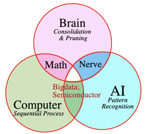
    • AIの利用は、1) 機械学習(ML)Algorithmに基づいてデータ収集し、判断や予測をする。2) 深層学習(DL) 特定データセットの分析と学習に基づくMLの一種 3) 自然言語処理 (NLP) 大量の自然言語データを処理・分析
  • トレーニングシステム推論システム:
    • AIトレーニングシステム:
      大量のデータセットにより特定活動の実施方法の学習アルゴリズムを進化させる。
    • AI推論システム:
      予め決められたモデルを使ってリアルタイムの決定を行う
  • AI関連技術の階層: (PWC)
    • アプリとサービス:
      資格処理、チャットボット、スマートアシスタント、アルゴリズム取引
    • プラットフォーム:
      機械学習、データ分析、NLP、Agent, Data solution を提供
    • (中間層) FTI (フレームワーク・ツール・インターフェース)
      開発者がモデルとアルゴリズムを設計・構築・販売できるようにするためのMLアルゴリズム、特定用途向けDL、トレーニング技術、多くはOSS
    • ライブラリ:
      特定HW上のAIフレームワークの配備に役立つ低レベルのSW機能。例: IntelのDL SDK/Vision SDK; NvidiaのcuDNN/TensorRT; ArmのNNがある。
    • ハードウェア:
      AI計算を最適化した処理装置と半導体論理回路。今後GPU, DSP, FPGA, Customised ASIC間での競争が激化。またAI HWを開発する企業数が従来のチップメーカー数を上回って増加している。
  • GAFAは自前のチップを制作し始めた。
    • Googleは、Deep Learningの処理用としてTPU (Tensol Processing Unit) を開発し、GPUより15-30倍高速で、30-80倍エネルギー効率がよいとされる。
      • これによりデータセンタの消費電力減らすことになる。TPUは、AlphaGoにも利用。
      • Google画像検索、Google翻訳、Google Cloud Vision APIなどに利用
    • Amazonは、データセンタに特化したAWS Graviton2というARMベースの高集積度のSoCを開発した。また家庭用Alexa向けAIチップを開発
    • Facebookは、IntelとAI用の消費電力の少ないチップを共同開発中
    • Appleは、米Intrinsityを買収し、ArmのCPU回路の高速化・省電化チップM1 (5nm)を開発した。
    • Microsoftは、スマートメガネHoloLens向けAIチップを開発
  • 今までは、半導体は電機製品の部品とされ、電機業界のニーズに応じた製品開発を行ってきた。
    • 今後は、ITサービス、インターネットサービスが通信効率の良いチップ開発を牽引している。
    • Claude Shannonの通信理論: 伝送効率C (bit/sec)は次の式で表される。
    • $C=W\log_2(1+\frac{S}{N})$
      W: 帯域幅、S:信号電力、N:ノイズ電力
  • AI市場での機会 (現在・将来): <左表
    • 計算、メモリ、保管、ネットワークの各分野でのAIに特化した (高速・省電力の)半導体の開発が期待される。
  • AI利用の機会をつかむ:
    • AIは、半導体産業にとって最大の推進力になることは確実。
    • 戦略とビジネスモデル
      • 今後、企業は現在の戦略ポートフォリオをAIフレンドリーに進化させるための方法を追求する。それには合弁や買収を含めた戦略的パートナーシップによるエコシステムの構築と有効活用が鍵となる。
      • ADASとIoTでのターゲット領域に注目
      • 半導体のような高度な技術を基礎とする産業には、まさにMOT (Management of Technology) が必須。プログラミング能力を技術と経営に活かす時代なのである。
    • 技術と製品開発
      • 正しい技術・アーキテクチャの追求
      • 脳神経プロセスによるDLアルゴリズムの深化
      • AIライブラリーとツールキット: SDKの深化
      • パートナーとの全面協力とエコシステム構築
  • デジタル・ビジネスモデル (RPOXM):
    1. カミソリと刃:
      • 主力製品を低マージンで、これに依存する追加商品を高マージンで提供する。
    2. プラットフォーム:
      • チップメーカと顧客の間のプラットフォーム参加者への利益をもたらすktrで、ホストは各種基準に影響を及ぼす。
    3. オープンソース:
      • OSSを通じた公開共有を通じてR&Dの分担と開発期間の短縮を狙う。
    4. XaaS:
      • インフラ、HW、SWの革新的サービスおクラウドサービス化することでサービス料として徴収
    5. マーケットプレイス:
      • 使用者の増加によるネットワーク効果を通じて市場価値を高め、開発者は新しいアルゴリズムとモデルをアップロードして充実させる。

>Top 10.
Optimal compute archirecture

Process speed HW interface Process
/Watt
Backward
compatibility
Flexibility Small size Tech capa
required
Low cost develop Proces/$ Training Inference

Language translation

GPU
ASIC
CPU
ASIC
Face detection GPU
FPGA
CPU
ASIC
Financial risk GPU
FPGA
CPU
Route optimization GPU CPU
Dynamic pricing GPU CPU
ASIC
Autonomous driving ASIC GPU
ASIC

FPGA
Comment
  • From: "Imitation Game, 2014 move": Alan Turing (1912-54) said that "sometimes it it the people no one can imagine anything of who do the things no one can imagine."
  • "Imitation Game, 2014 映画": Alan Turing (1912-54) の言葉
    "時々、想像さえしない誰かが、誰も想像したことのないことをやってのける。"

| Top | Home | Article | Bookshelf | Keyword | Author | Oxymoron |